We capture the future with innovative technology.
Since 2003, in the field of Surface-Mount Technology (SMT), we have mass-produced a diverse range of mixed-size components (from 0402 chips to 88mm odd-shaped materials, Stick (bulk), Tray ICs, etc.), applied lead-free production capabilities and reliability assessments. In the IMT sector, we have ensured customer quality and reliability through Wave Soldering, In-Circuit Testing (ICT), Functional Circuit Testing (FCT), coating, firmware inspection, aging tests, and thermal shock assessment. For the growth of the SMT technology sector, we are actively expanding our micro-assembly technology (0201 Chip, 0.3mm Ball) and mixed assembly techniques. We are committed to providing global solutions by integrating Smart Factory, automation, and robotics technologies.
Securing mass production capabilities through optimal management of printing, placement, and curing conditions on ceramic substrates, along with traceability and timely inspection management system, ensuring reliability through shear and thermal shock assessments, operating a Clean Room (class 3,000), and obtaining water-soluble solder printing, placement, and cleaning technologies for semiconductor and medical device cleaning; moreover, we pursue a One Stop Service through SMT, IMT, ICT, FCT, coating, aging, and assembly processes.
SMT, IMT Business Expansion
Total Poduct Quantity
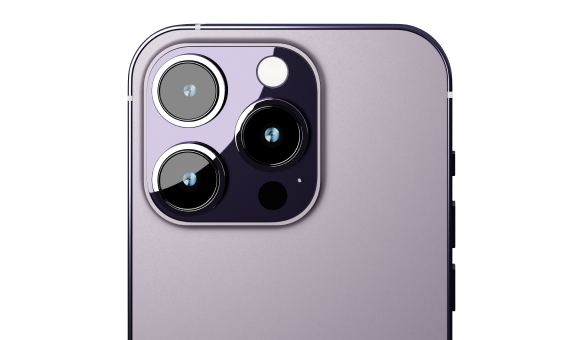
We produce circuit boards with precision component
placement required for the operation of high-performance and
multifunctional camera modules (high-resolution/optical zoom,
autofocus, optical image stabilization) applied in smartphones
and tablets, as well as 3D sensing modules (such as 3D depth
and distance measurement of subjects).

Securing technology for printing, mounting, and curing of 0201 chips and 0.3mm BGA balls on ceramic substrates

Traceability and timely inspection management system via QR Code

Operation of Clean Rooms for reliability assurance, as well as component shear strength measurement and thermal shock testing.

Acquisition of water-soluble solder printing, mounting, and cleaning technologies
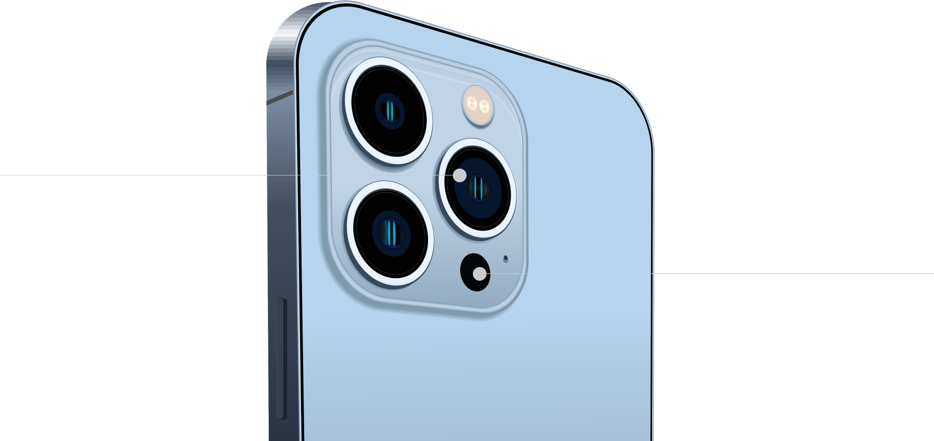
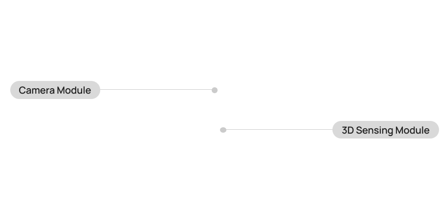
Camera Module
3D Sensing Module


 TOP
TOP


